NVIDIA and TSMC Deploy Shocking New AI Inside Advanced Fabs
NVIDIA and TSMC are integrating advanced AI models directly into fabrication facilities to solve complex next-generation semiconductor manufacturing challenges.
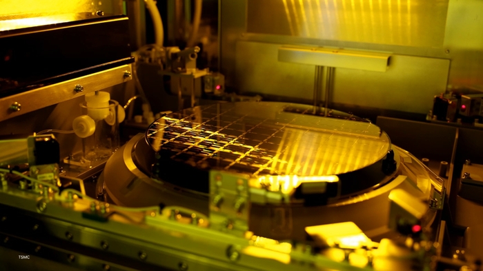
The modern technology landscape is hit by a massive shifting paradigm. As hardware engineering pushes past traditional scaling limits, building the physical processors that power our daily lives has transformed into one of the most mathematically exhausting tasks in human history. The old methods of printing circuits onto silicon are no longer enough when dealing with angstrom-level components.
In a massive announcement breaking directly out of the NVIDIA GTC Taipei event, NVIDIA and TSMC (Taiwan Semiconductor Manufacturing Company) revealed a deep technical partnership aimed at embedding accelerated computing and artificial intelligence straight into the physical microchip manufacturing pipeline.
As consumer demand surges for high-performance graphics hardware—such as the desktop-class components squeezed into the massive ASUS ROG Strix Scar 18 ,the factories responsible for creating this silicon are hitting severe computational bottlenecks. To bypass these physical limits, TSMC is actively deploying NVIDIA’s CUDA-X libraries and specialized vision AI models across its entire advanced lifecycle, including computational lithography, transistor simulation, and advanced process control.
Technical Overview: The Embedded AI Stack
To truly appreciate how deeply integrated this software deployment is, we can look at the specific accelerated libraries and toolkits TSMC is running inside its multi-billion-dollar fabrication plants (“fabs”):
| AI Framework / Library | Primary Operational Role inside the Fab | Real-World Performance Impact |
| NVIDIA cuLitho | GPU-accelerated computational lithography mask design | 20% to 50% improvement in cycle times |
| NVIDIA cuEST | GPU-accelerated electronic structure simulation for materials | 50x faster average chemistry simulations |
| NVIDIA Metropolis | Vision AI framework for automated video and pixel tracking | Drastically slashes structural defect escape rates |
| NVIDIA TAO Toolkit | Low-code AI model training and optimization pipeline | Minimizes manual data labeling and retraining loops |
| NVIDIA Omniverse FabTwin | Digital twin physics-based factory simulation ecosystem | Maps real-time process variations across production floors |
1. Rewriting the Physics of Printing: NVIDIA cuLitho
At the very foundation of chip manufacturing is a process called computational lithography. This is essentially the printing method used to create complex photomasks that dictate where billions of microscopic transistors sit on a wafer.
Historically, calculating the way light waves bend around sub-nanometer mask shapes required massive, power-hungry server farms running on traditional central processing units (CPUs). This single step stands as one of the largest computing workloads in the entire semiconductor industry.
By transitioning this work onto GPU-accelerated clusters running NVIDIA cuLitho, TSMC has unlocked a game-changing efficiency boost. Calculations that used to take weeks to compute can now be completed overnight.
According to official engineering logs, the system provides a 20% to 50% improvement in cost-effectiveness and factory cycle times compared to legacy CPU methods, all while keeping the exact same operational cost of ownership. This rapid turnaround ensures that next-generation microarchitectures move from testing phases into retail boxes faster than ever before.
2. Advanced Vision AI: Detecting Nanometer Defects
When managing production lines running 24/7, catching structural anomalies early is vital to maintaining healthy factory outputs. Even a single speck of microscopic dust or a minor laser misalignment can ruin an entire batch of expensive wafers, sending thousands of potentially elite gaming processors straight into the scrap bin.
To fight this, TSMC is employing the NVIDIA Metropolis framework alongside the TAO Toolkit to advance its automated defect inspection workflows with state-of-the-art vision AI. Older automated optical inspection machinery relied heavily on human operators to manually look at flags, categorize rare defects, and constantly retrain statistical models.
The new deep-learning models train themselves to spot nanometer-scale defects on the fly. This minimizes the need for repeated manual labeling loops and lets the system evolve dynamically as newer, more intricate node variations are rolled out onto the main production floors.
3. Molecular Mastery: 50x Faster Material Simulation via cuEST
Before a factory can print a circuit, materials scientists must spend months studying the molecular and chemical properties of new silicon substrates, chemical washes, and protective coatings. This realm of electronic structure simulation requires deep quantum chemistry mathematics.
Under the newly expanded framework, TSMC is adopting NVIDIA cuEST. This library accelerates complex chemical and structural physics simulations via modern graphics architectures.
The real-world math is stunning: cuEST delivers an average 50x speedup for chemistry simulations. This means research groups can model how molecules behave under extreme lithographic heat in a matter of hours rather than waiting days for older server architectures to finish processing the datasets.
The Broader Impact on Premium Hardware and Gaming
While software optimization inside a factory in Taiwan might seem distant from everyday consumer technology, this structural evolution directly impacts the availability, pricing, and capabilities of the devices sitting on your desk.
Driving Down Hardware Failures
When a foundry suffers from poor structural yields, the cost of manufacturing skyrocketing components gets passed down to the consumer. By pushing down error margins and cutting lithography cycle times, this AI-driven approach helps keep production steady.
This directly aids the production of high-end consumer gear. Whether you are tracking the complex audio processing loops found in the custom drivers of our Logitech G Pro X 2 Lightspeed review, or measuring the processing power required to drive premium displays like the classic panel inside the LG G6 review, everything relies on the foundational efficiency of advanced semiconductor fabrication.
The Verdict: A New Operational Gold Standard
As Jensen Huang, founder and CEO of NVIDIA, accurately framed the partnership:
“TSMC is bringing NVIDIA AI and accelerated computing into the fab itself, tackling some of the world’s most complex design and manufacturing challenges with simulation, optimization and AI to improve speed, efficiency and yield for the next generation of chips.”
The collaboration between NVIDIA and TSMC represents a spectacular leap forward for global hardware scaling. By utilizing software intelligence to solve hardware physics limits, they aren’t just making factories faster—they are paving a reliable path forward for the next decade of supercomputing.
For a deep technical look at how these newly manufactured chips run inside high-end user rigs, be sure to check out our comprehensive ASUS ROG Strix Scar 18 Performance Analysis to see what happens when unrestricted power meets bleeding-edge display tech.
What do you think?
Do you think using artificial intelligence to build physical computer components will help solve global hardware shortages, or are we making the supply chain too reliant on automated software? Let us know your thoughts in the comments below!